Solar Cell Fabrication
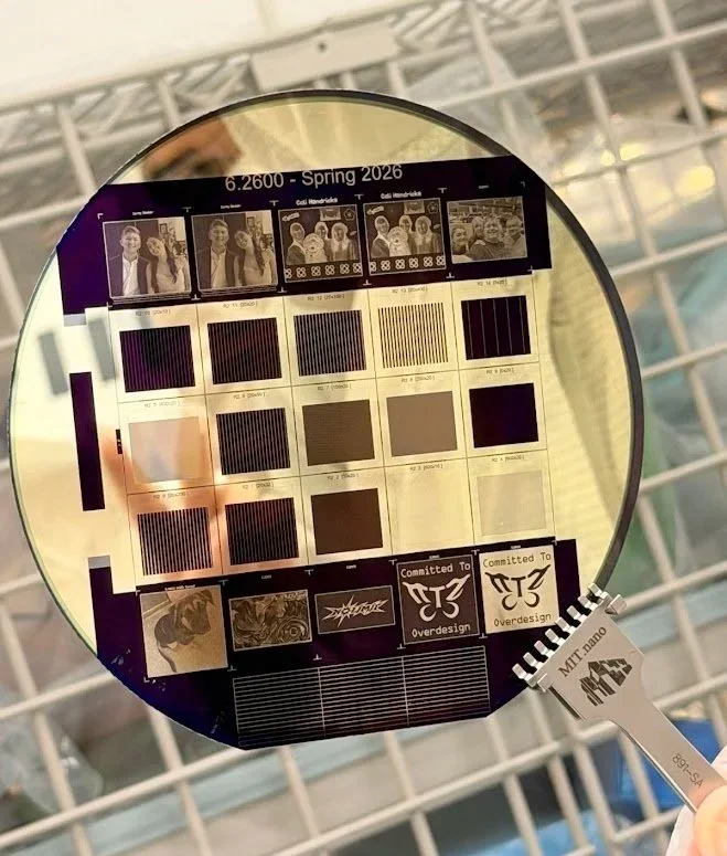
Final Si Wafer Exposed/Developed/Etched Designs.
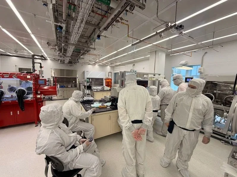
I’m taking 6.2600 (Micro/Nano Processing Technology) this semester. It’s one of the most interesting classes I’ve taken - we get to go into the clean rooms of MIT.Nano, learn fabrication techniques and use some really sophisticated characterization tools. The first portion of the class is devoted to understanding the steps and physics fundamentals behind creating solar cells.
The class also includes a scientific communication component, where we focus on honing our ability to explain complex technical concepts to an audience with minimal knowledge.
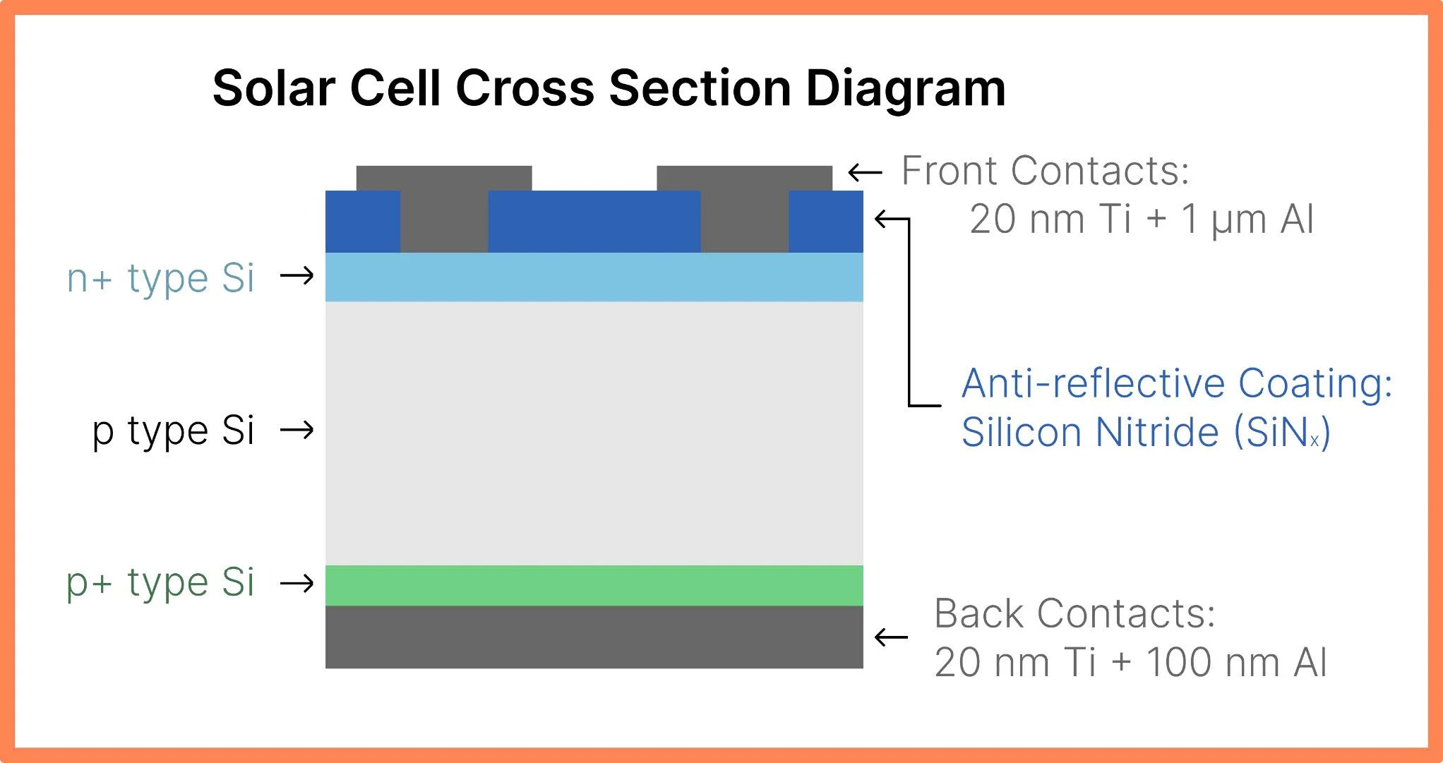
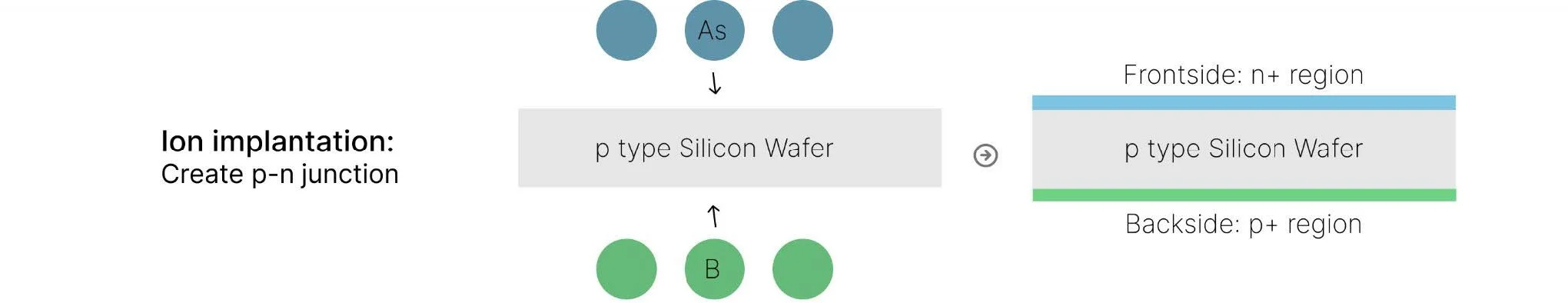
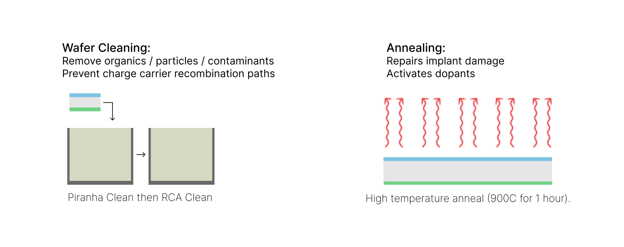
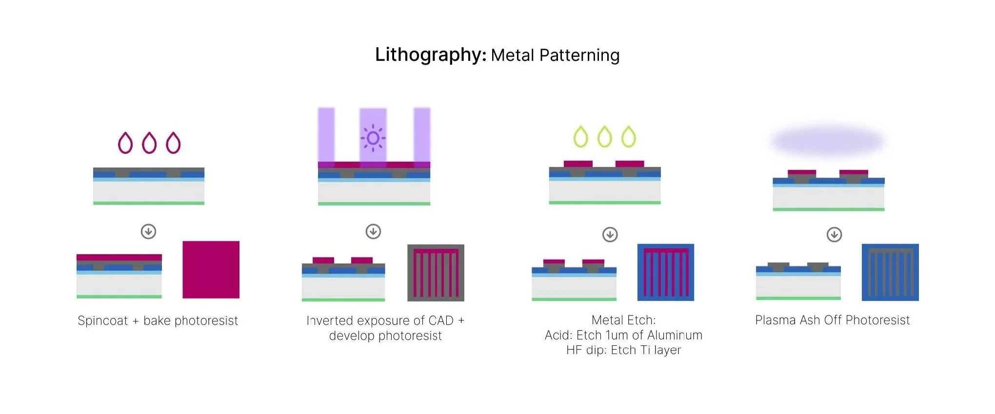
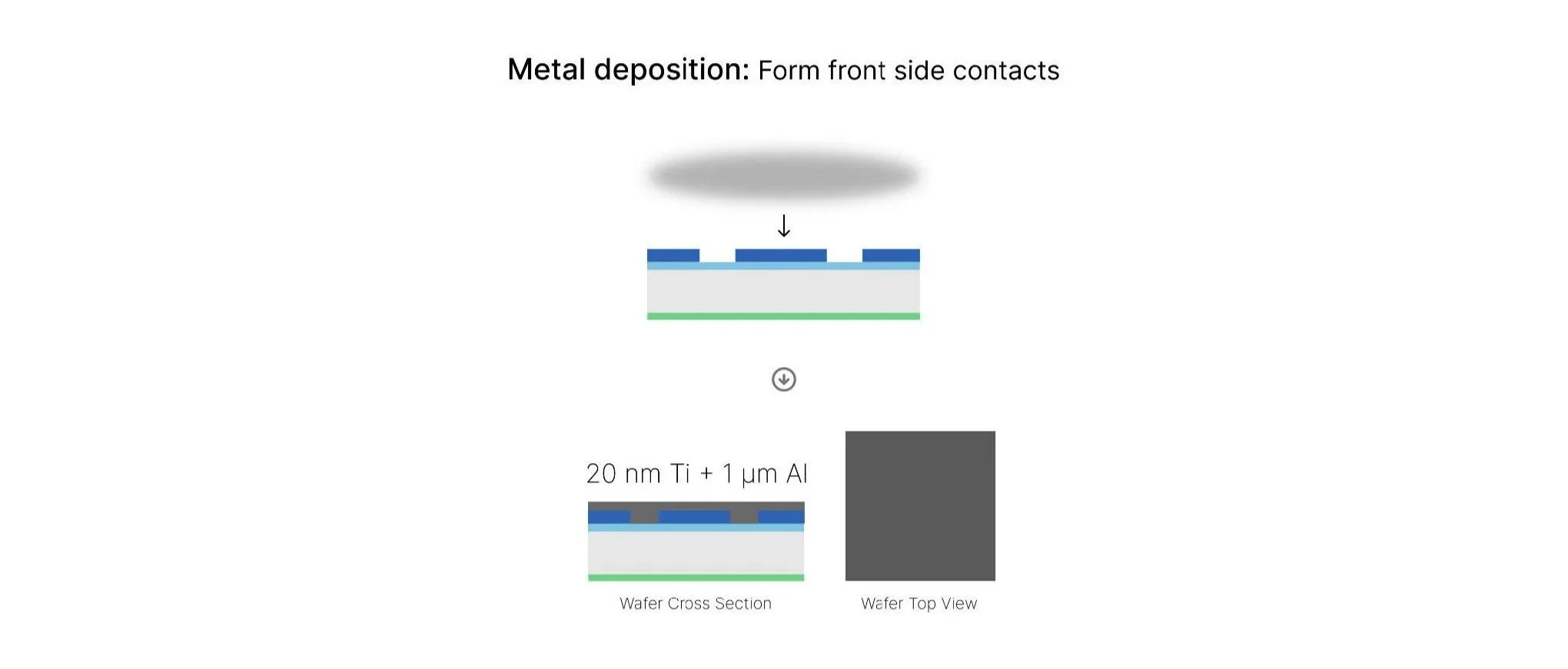
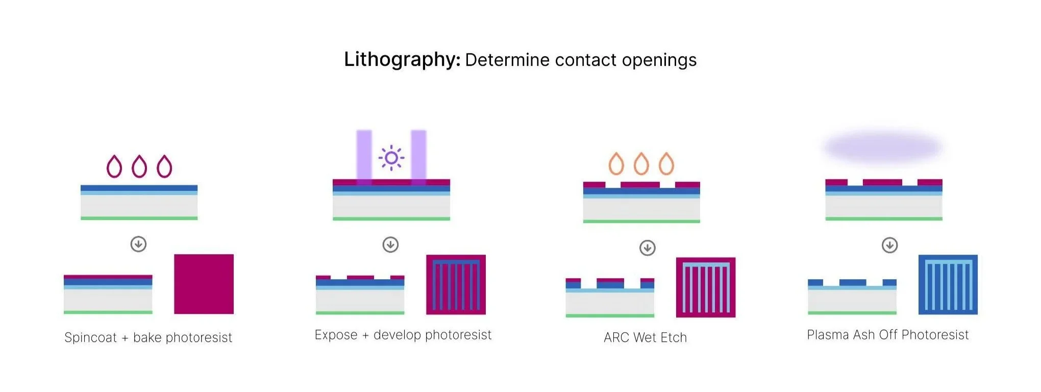
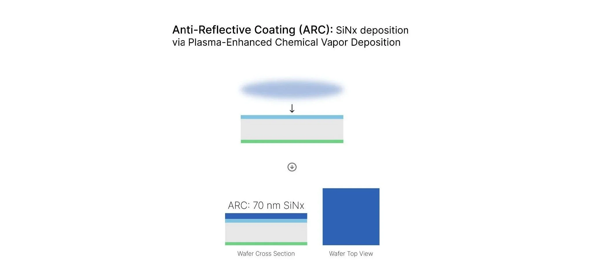
I’m also trying to build up my Figma skills these days, so for our first presentation, I created custom minimalist graphics that explain the solar cell fabrication process.
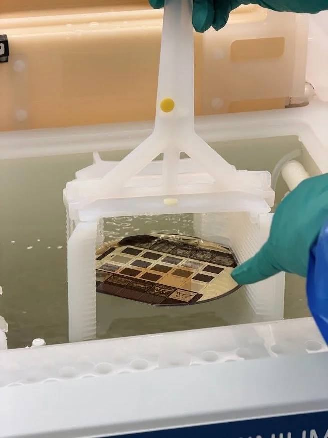
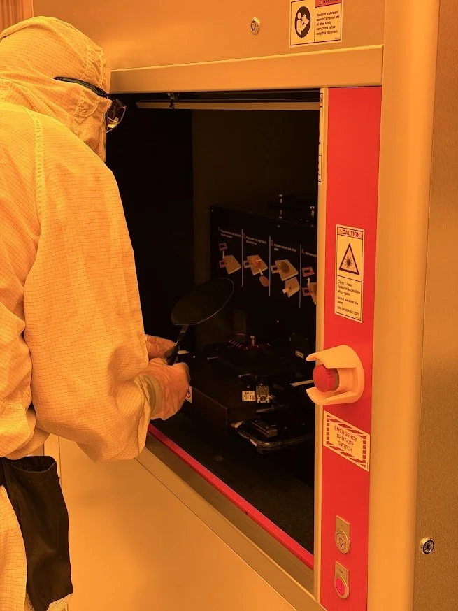
HF Dip (One of many wafer cleaning steps)
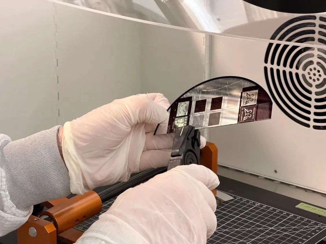
Manual Wafer Cleaving (terrifying, I broke one)
Characterizing Solar Cell Efficiency
Using the MLA Direct Write (Photoresist exposure)
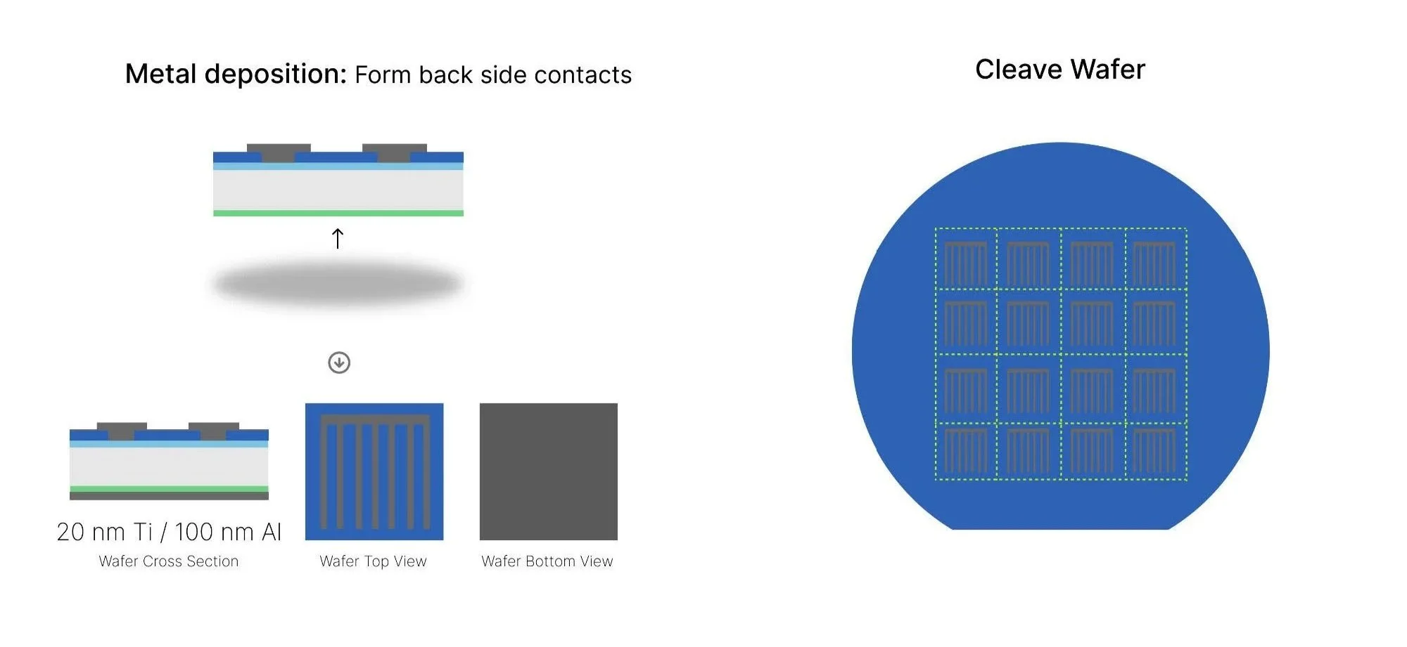
Solar Cell Fabrication Graphics
Solar Cell Presentation
This is my group’s solar cell presentation, showing the fabrication, characterization, and analysis we carried out across 15 solar cell designs.